CMOS Image Sensors: Evolution, Patent Trends, Leading Players & More
Image sensors are semiconductor devices used to capture the world with a touch of our fingers. Thanks to the evolution in semiconductor technology, the size of image sensors has also reduced to the tip of our fingers. It is estimated that over 1.7 trillion images will be taken in 2022. This is a testament to the widespread role image sensors have in our lives. These sensors can now capture details on macroscopic and microscopic levels that not even a human eye can capture. The primary function of the image sensor is to capture light from our environment and convert the captured light into electrical signals. Image sensors can be categorized into Charge-Coupled Devices (CCD) and Complementary Metal Oxide Semiconductor (CMOS) image sensors based on the architecture for converting light to electrical signals, and device structure. The latter are used in all sorts of digital cameras for image and video shooting.
This article will discuss the evolution of image sensors from CCD to CMOS, their main components and advantages, applications, the difference between the front-side and backside illuminated CMOS image sensors, major players in the market, and top patent assignees in the image sensor technology.
Table of Contents
A Brief History of Image Sensors
MOS image sensors are not a recent development. They were first devised and developed in the mid-1960s when the existing technology for capturing images and video was the vidicon tube. However, despite the excellent image quality, there were several downsides, such as its large size, lagging video, and huge weight. In addition, it also suffered from temporal noise and high fixed patterns.
CCD image sensors were developed in 1969 to overcome the problem of MOS image sensors, and they quickly captured the market. All pixel charges in a CCD sensor are transformed to an analog voltage, amplified, and digitized via an output. Throughout the 1970s, the use of MOS image sensors had been restricted to a few particular applications, such as spectroscopy, and CCD ruled the image sensors market because of its inherently lower fixed-pattern noise (FPN). However, there was one problem: the CCD market was controlled by only a few companies, which created a conducive environment for research on CMOS image sensors (CIS) by universities and companies.
The downside of CCD image sensors, such as high energy consumption, the slow reading speed of the serial data stream, low homogeneity and quality of image, poor link performance, and low battery life, were overcome by CIS. Each pixel undergoes a charge/voltage conversion in a CIS, and the image data is transformed into digital data on the CMOS sensor chip. This advantage of parallel read-out of picture data from a CMOS sensor offers a higher frame rate at comparable resolutions.
A CIS has a smaller analog to digital conversions (ADC) per pixel column than CCD, enabling faster frame rates. CMOS sensors have improved dramatically over the years, and the most recent ones are now equivalent to or better than CCD in terms of image quality, image speed, and total value. In addition, the CMOS image sensors enable scalability by allowing image acquisition and processing circuitry to be integrated on the same chip using a standard CMOS process.
Now that we are aware of the history of image sensors and the evolution of CIS, let us discuss its main components that contribute to an excellent performance.
Critical Components of a CMOS Image Sensor
There are four essential components in a CMOS image sensor, as shown in Figure 1.
- Microlens
- Color Filter (CF)
- Transistors and Interconnects
- Photodiode (PD)
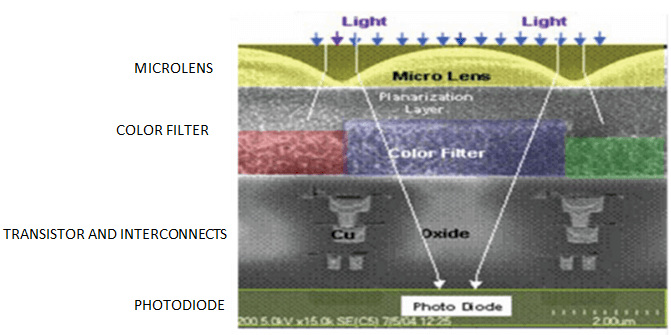
A CIS comprises an array of microlens used to direct light towards the photodiodes. The RGB (red, green, and blue) components of directed light are separated using the color filters. The photodiode (PD) is a device that collects photons/captures light and converts the collected photoelectrons into electrical signals. The pixel transistors are used for controlling the signals that are transported within the image sensor using interconnect structures/metal wiring. The CMOS image sensors can be categorized into Front-Side Illuminated (FSI) and Backside Illuminated (BSI) based on the placement of the photodiode and interconnects layers concerning each other.
In the next section, we will discuss the advantages of CMOS sensors over CCD image sensors.
Advantages of CMOS Image Sensors
There are numerous advantages of using CMOS image sensors over CCD image sensors. The four main advantages have been discussed below:
- Energy consumption is significantly reduced in a CMOS image sensor. It is crucial as less heat dissipation means a more excellent camera with less noise.
- It has higher sensitivity owing to the new pixel architecture, which is helpful in low-light situations. Sensitivity in the near-infrared band and short-wave infrared radiation is heightened.
- A better fidelity image will benefit from less dark noise.
- The camera size can be smaller because the read-out logic may be built into the same chip.
The advantages of a CMOS image sensor can be better understood when we capture its differences from a CCD image sensor. These are highlighted in Table 1 below:
| CHARACTERISTICS | CCD IMAGE SENSOR | CMOS IMAGE SENSOR |
| Type of signal from pixel | Electronic packet | Voltage |
| Type of signal from chip | Analog voltage | Bits (digital) |
| Read-out noise | Low | Comparatively lower at equivalent frame rate |
| Fill Factor | High | Moderate or low |
| Photo response | Moderate to high | Moderate to high |
| Sensitivity | High | Comparatively higher |
| Dynamic range | High | Moderate to high |
| Uniformity | High | Comparatively lower |
| Power consumption | Moderate to high | Low to moderate |
| Shuttering | Fast and efficient | Also fast and efficient |
| Speed | Moderate to high | Relatively higher |
| Windowing | Limited | Multiple |
| Anti-blooming | High to none | Always high |
| Image artifact | Smearing with charge transfer efficiency | FPN, Motion electronic rolling shutter(ERS), parasitic light sensitivity (PLS) |
| Biasing and clocking | Multiple with higher voltage | Single with low voltage |
| System complexity | High | Relatively low |
| Sensor complexity | Low | Comparatively high |
| Relative R&D cost | Low | Low or high, depending on the series |
To further better the performance of CIS, some changes had been made in the arrangement of its components for a shift from the front-side illumination to the backside illumination. In the next section, we will understand the difference between the workings of the front-side and backside-illuminated CMOS image sensors.
Front-Side Illuminated (FSI) Versus Backside Illuminated (BSI) CMOS Image Sensors
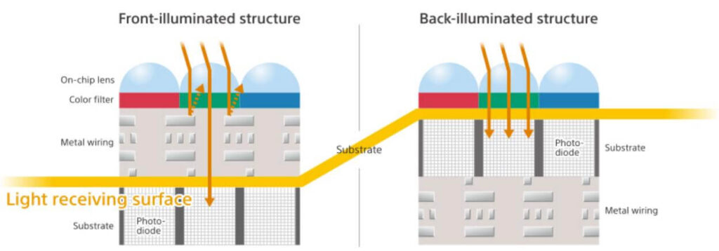
The working of FSI and BSI CMOS image sensors are shown in Figure 2. The conventional CMOS image sensors follow front-side Illuminated (FSI) architecture with a microlens array at the top, followed by color filters, interconnect layer below color filters, and the photodiodes at the bottom. In FSI image sensors, light enters pixels through the front metal wiring and concentrates on the photosensitive region (photodiode). Since the ratio of the height of the pixel’s optical stack and the pixel size is minimal for larger pixels, the photosensitive area is relatively guaranteed. Therefore, the FSI image sensors have a better performance for larger pixels.
As the industry strived to reduce the size of the CMOS image sensors or increase the number of pixels in a given area to improve resolution, there was a call to shrink the pixel size. Unfortunately, the pixel size shrinkage led to reduced fill factor, longer optical route, and loss in the absorption of metal wiring’s light, lowering the FSI sensor’s performance.
The BSI (Backside Illuminated) architecture resolved the problem by placing the photodiode layer at the top of the interconnect layer. It separates electrical components from light, allowing the optical route to be tuned independently, eliminating the FSI metal wiring layer’s absorption, reflection, and flare. Furthermore, the BSI pixel’s optical stack is considerably reduced and achieves a higher QE (quantum efficiency) than FSI.
BSI for Present and the Future
The need for the evolution of the image sensors is either to improve their performance or to reduce their size.
The BSI sensors evolved to stacked sensor structures that include the pixel layer formed over a chip in place of the supporting substrate in conventional BSI sensors. The stacked sensor structures enabled the mounting of large-scale circuits on a small chip. Since the pixel and circuit sections are formed on a different chip, specialized manufacturing processes are used to produce a pixel section with high image quality and a circuit section with high performance, enabling higher resolution and a compact size.
These stacked BSI structures utilized through-silicon via (TSV) in the pixel array’s periphery to provide connections between the pixel and circuit die. It led to the development of Cu-Cu direct bonding between the stacked pixel and circuit dies which enabled space-saving around the periphery and reduction in the size of the sensors.
The focus on autonomous vehicles has led to significant research and development in aspects, such as Time of Flight (ToF), single-photon avalanche diode (SPAD) pixels, and the use of AI within image sensors. The ToF and SPAD enable measurement of the distance of an object (e.g. vehicle, person, road sign, etc.) from the detector, while AI enables faster processing of the captured image for pattern/object identification within the sensor.
Higher resolution, minimum power consumption, and lower costs benefit smaller pixels in CMOS image sensors. These benefits remain the factors for the current and future advancements in the CIS technology, and are expected to boost the market growth.
Due to their many benefits, CMOS image sensors find practical applications in many industries and devices. Therefore, our next point of discussion will center on its real-world applications.
Application Areas of CMOS Image Sensors
The CMOS image sensors have many application areas, including mobile, computing, security, medicine, automobile, and defense. The incorporation of camera systems in mobile devices and the continuous increase in demand for smartphones by consumers have led to the drastic evolution of image sensors. The image sensors remain an area of constant development for providing high-quality images while reducing the size of the sensor module within smartphones. In addition, smartphones utilize image sensors for a range of security applications that enable user authentication, such as facial recognition, in-screen fingerprint recognition, iris recognition, etc.
CIS has recently found a significant application in the automotive industry based on the work in the field of autonomous vehicles that utilize an array of image sensors for implementation of Driver Monitoring Systems (DMS) and Advanced Driver Assistance Systems (ADAS).
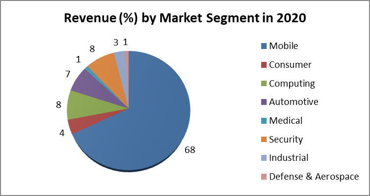
The image sensors also have applications in drones, robots, virtual reality, augmented reality, mixed reality, and gesture-based gaming consoles. Figure 3 lists the revenue percentage by market segments of CMOS image sensors in 2020. Mobile comfortably led the race with a 68% share, followed by computing and security at 8 percent each.
Considering the wide array of applications, each with its own set of requirements from the image sensors, there is an inherent need for evolution in the technology. These application areas have led to the CMOS image sensors capturing a market size of almost $21 billion in 2020, which will continue to increase. Let us look at some of its key market trends in the next section.
Key Market Trends in CMOS Image Sensors
- CMOS image sensors have many applications in smartphones, tablets, and digital single-lens reflex (DSLR) cameras. As the smartphone manufacturers focus their attention on improving the camera quality, the demand for CIS is expected to be steady in the coming years.
- In addition, the inclination toward dual-camera smartphones by all major smartphone vendors due to consumer preference is expected to help sustain demand. The underlying technology used in dual-camera smartphones requires two sensors. Together, they combine the colored and monochrome images generated by the individual CMOS image sensors to create a single image. Now even twin cameras are not enough for consumers as Galaxy S22 Ultra from Samsung boasts five cameras, four rear, and one front camera.
- The consumer’s preference for dual and 3D cameras will significantly impact CMOS volumes. In addition, new applications, such as telescopic lens drones, virtual reality, robots, and augmented reality, are anticipated to fuel this rising market.
- Consumer electronics consumption has been on the rise globally. According to the National Bureau of Statistics of China, the retail trade revenue of consumer electronics and household appliances in China stood at CNY 96.31 billion in June 2019 alone. A number of camera-equipped electronic goods are projected to drive the market for CMOS image sensors.
- The Asia-Pacific region is anticipated to drive the market in the next few years. China is anticipated to lead the growth because of its burgeoning middle class and demand for consumer electronic goods. As per the data of the National Bureau of Statistics China, the country’s electronic equipment, communication equipment, and computer manufacturing market increased by 13.1 in the fiscal year 2018.
- Thanks to government initiatives, India is also experiencing steady growth in several smart cities projects. The increase in smart cities projects will power the demand for CMOS image sensors as the need for electronics solutions, such as surveillance, monitoring, and maintenance, will assume a central role.
- The CMOS Image sensors will also find practical applications in the healthcare industry as non-invasive testing equipment for scanning purposes. The healthcare industry in India is anticipated to reach approximately USD 133 billion by 2023.
- The Asia-Pacific region is also projected to contribute to more than 25 percent of the global smart homes by 2030, and the sales are expected to jump to USD 120 billion. At present, Japan is leading the race. However, the push toward adopting smart homes will accelerate the demand for CMOS image sensors in the region.
To have a better insight into the current and future state of the CMOS image sensor market, we will focus our discussion on its leading players across the globe.
Major Players in the Global CMOS Image Sensor Market
Key players, such as Sony, Samsung, OmniVision, and ST Microelectronics, continue to invest in the development of technologies that would give them an edge over the competition. The name of the leading players by market share occupied is shown in Figure 4 below:

- Sony: It has recently developed stacked CMOS image sensor technology with 2-layer transistor pixels. The conventional CMOS image sensors’ photodiodes and pixel transistors occupy the same substrate. Sony’s new technology separates photodiodes and pixel transistors on different substrate layers. This new architecture approximately doubles the saturation signal level in comparison to conventional image sensors, widens the dynamic range, and reduces noise, substantially improving imaging properties.
- Samsung: The company recently launched ISOCELL HP1 image sensors based on ChameleonCell technology. The ChameleonCell technology enables pixel-binning that uses a two-by-two, four-by-four, or complete pixel layout depending on the environment (i.e., low-lit or bright). In a low-lit environment (e.g., indoors or in the evening), the HP1 transforms into a 12.5MP image sensor by merging 16 neighboring pixels, which captures brighter and clearer photos. The sensor’s 200-million pixels can capture ultra-high-definition photography on mobile devices in bright environments.
- OmniVision: It recently announced a significant pixel technology breakthrough in developing the world’s tiniest 0.56-µm pixel with high quantum efficiency (QE) performance, excellent quad phase detection (QPD) autofocus capabilities, and low power consumption. With a pixel size that is smaller than the wavelength of red light, the pixel shrink is no longer constrained by the wavelength of light. The pixel is based on OmniVision’s PureCel®Plus-S stacking technology, and deep photodiode technology is applied to embed the photodiode deeper into the silicon carefully. These advanced technologies have enabled OmniVision to develop the tiniest pixel, allowing for higher resolutions in the same optical format and further enabling the image sensor to have more ISP functions, lower power consumption, and faster read-out speed.
- SK Hynix: The Company recently unveiled a new technology called the All 4-Coupled (A4C) image sensor that provides a giant leap forward from the conventional Phase Detection Auto Focus (PDAF). The A4C uses a photodiode to convert light into electric current and color filters to absorb specific light wavelengths selectively. The A4C structure has one microlens on each group of four-color filters of the same color pixels enabling faster and more accurate focusing of a subject using the different rays of light from the subject to converge to one focal point.
A quick analysis of the assignees (as shown in Figure 5) to one of the CPC classes – H01L27/1464 specific to BSI sensor structure – shows that the key players capturing significant market share for image sensors are also some of the top patent filers in the field of BSI. Sony, Samsung, and OmniVision are leaders in developing the BSI technology while holding most of the market share for image sensors.

Conclusion
We can say that CCDs found a thriving market for video cameras and DSC (Digital Still Cameras). However, the development in the technology and the demand for CIS for smartphones enabled CIS to also be used in video cameras and DSC that required good image quality with faster processing. It has led to the shrinking of the market for CCD image sensors and expansion in the market for CIS. The requirement for higher resolution, smaller pixel size, and higher QE led to the emergence of BSI. The BSI technology continues to evolve based on widespread applications with specific requirements.
It is crucial to stay on top of the technology curve to have a competitive edge in the business. Patenting your idea and invention is an excellent way to assert your presence in the market for new technology. Many companies with optimal resources perform the task of securing patent grants themselves. However, the task becomes challenging with multiple players attempting to receive a patent grant for the same invention. That is why the services of a third party with proven capabilities are valuable.
Sagacious IP is a global IP research and consulting company. Since its inception, its focus has been to leverage its profound capabilities to deliver world-class IP solutions for its clients. Its unique approach has garnered appreciation from different quarters of the industry. In addition, through its technology scouting services, it assists organizations in spotting promising trends in the CMOS image sensor domain. Click here to know more about this service.
– Kushagra Magoon (ICT Licensing) and the Editorial Team
Having Queries? Contact Us Now!
"*" indicates required fields